I have received intelligent criticism, which I feel honored and proud to have received. It would be easier to reply and follow threads if whoever posts comments "signs" them with a nickname, such as "Last Mohican" or whatever.
My responses:
Received from "Third Factory..."
Errr... 3rd factory? (I though it was replacing an existing factory - that would make 2)
Your analysis on capacity is way off, several obvious issues:
1) you assume F36 will be double the output of F30 - that would be true IF they both had same wafer starts/month (which they don't) AND 300mm has same yield as 200mm - I haven't seen any data that 300mm yield = 200mm yield for AMD.
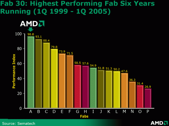
Who has seen the data you are demanding?. There is no reason to think that yields have to be lower at 300mm, they could, but I would like to know possible reasons. Same thing about the number of wafer starts. Under the reasonable assumption of other things equal, the fact is that 300mm wafers have 225% the surface of 200mm wafers, thus, Fab36 should be, eventually, in conditions to supply, all on its own, 40% of the market, because Fab30 supplies 22%.
AMD prides about lots of accomplishments such as running test wafers next to production ones in the same lines. I am willing to be optimistic and assume that the disrruption of the retrofitting Fab30 will be light.
2) I believe <10% of AMD's current production is dual core, as they migrate more to dual core they will get fewer die/wafer (unless of course they continue to plan to only make 10% dual core...) And any quad core production will cut into capacity even further. That cuts the legs out of your 300mm will provide 2X the dies of 200mm argument (it will be ~same if you account for migration from single to dual core) 3) The conversion of F30-F38 will actually limit their production during that conversion to <2 fabs
[...]Another thing to keep in mind is 300mm automation and material handling systems are completely different so it is not just a matter of swapping 200mm tools for 300mm tools. FYI - 200mm-300mm conversion is not "radical upgrading"; numerous IC manufacturers have done this.So, you are saying that the equipment is totally different and the transition is not radical (!?)
Another anonymous post:
Yes, I made that mistake. Do you find it particularly relevant?
Just a (few) problems with your knowledge of process technology:
"The transition to 65nm was neutered by AMD's 90nm sSOI; pushing them further down the path toward 42nm."
It's 45nm, I thought it may have been a typo until you repeated it again.
Your other link says: "The wires are thinner, the resistance is higher, the lost power greater."The "other link" should refer to "Intel's 65nm is just marketing"
I don't say they do. I was just illustrating an idea, that the transition to ever smaller transistors incurrs in trade-offs in which things that used to be negligible are not anymore.
Ummm... the major power deltas between 90nm and 65 nm is off state leakage casued by leakage between the gate and channel and from source to drain (neither of these have anything to do with "tiny wires". Also SOI doesn't impact either of these - the main
That is your opinion, and most definitively not authoritative. Googling SOI I found studies that prove SOI to be more than cost effective.
benfit of SOI is latch up protection which can be minimized much more cheaply with better implant processed. (SOI adds at least 10-15% to production cost of a wafer)
"APM, a robotic tech. for chips production"
Do you actually think APM has or uses robots? It is just a SW control system - all other
 Sure, I think it is Rosie, of the "Jetsons", the female maid robot (Robotina de los Supersónicos para los panas hispanohablantes) who made AMD to win the best factory award by Sematech for years and years (as mentioned by Daryl Ostrander here, slide #17 of 28). But of course, you are entitled to think that AMD is like Intel in which the manufacturing process is controlled not by robotic technology but "Copy Exactly!"ing the factories. Are you going to say that is as flexible as AMD's? Anyway, I am not scared to acknowledge that I misused "robotic" to refer to Automated Production Manufacturing, but it is implied that the machines intervening, since they are computer controlled, qualify as robots.
Perhaps I am wrong, but in my ignorance, I have seen a lot of people referring only to the benefit of the smaller size, that is, half the "variable cost" of production, ignoring the outstanding capital investments of retooling for more detailed silicon processing, or the "fixed costs". And by the way, the yields *do* take a hit
the major manufacturers use their own systems (TSMC, Intel, Samsung, etc) - it is impossibel to compare the systems as none of the companies disclose the specifics of how and what they do.
"First fallacy: It is cheaper to manufacture the same number of transistors at 65nm than 90nm"
As you get roughly double the transistors your yield rate would have to go by a little less than a factor of 2 for it to be cost neutral (the reason it is less than 2 is that there are additional manufacturing steps and 1 metal layer which adds cost to the 65nm process. Your analysis is not congruent with your statment as you are comparing an older technology on single core (or 1/2 cache) to the newer technology with dual core or (double the cache). Your statement above says same number of TRANSISTORS (the
65nm example you give has many more transistors, thus you are comparing apples to oranges)
I'm not sure what you're background is in, but it is clearly not semiconductor process tecnhnology or manufacturing.
You are right about that last one; although sincerely you make me wonder whether you are even more ignorant ;-)
From "Bears run to cover":
Please explain to me how SOI minimizes the amount of leakage between the gate in a transistor and the channel (which are spearated by a 12A gate oxide)? Hint - it doesn't.
Please explain to me how SOI prevents lekaage between the source and drain (which is separated by the Si channel)?. Hint - It doesn't
SOI does not have significant impact on leakage - the reason between Intel P4 and AMD K8 power is chip design and clock frequency! Hence, Conroe which has much lower clock frequency than the P4's has a much lower TDP on the same manufacturing technology.
The only leakage path SOI addresses is junction leakage which is a distant third to gate leakage and source-drain leakages.
You may call me superficial, but wikipedia disagrees with you:
Silicon on insulator (SOI) is a layered structure consisting of a thin layer of silicon, from 50 nm to 100 µm, which is created on an insulating substrate, which is usually sapphire or silicon with an insulating layer of silicon dioxide(SiO2) 80 nm to 3 µm thick on its surface. This process reduces the amount of electrical charge that the transistor has to move during a switching operation, increasing speed (up to 15%) and reducing switching energy (up to 30%) over CMOS-based chips. SOI chips cost more to produce and are generally used for high-end applications. [my emphasis]
Switching power loses are the most significant at these speeds and feature sizes.
Another anonymous, from the same article:
Fanless: Can use just a passive disipator: No noise, no mechanical parts that wear down and deteriorate
Some questions:
1) what is the major source of noise in a computer?
2) what is the failure rate for a CPUY fan; based on your comment above this is an important factor?
Let's see, in *my* computer, it is not the harddrives (I buy the quiet ones), it is not the Floppy (which I don't even have ;-) it is not the DVD drive (which I seldomly use), it is definitively not the network connection. It is the power supply fan!. Now, if I had a "Rackable" computer, one of those which has the power transformer outside the computer, or if my computer were powered by the twisted pair cable as some routers are, guess what: It would be **me** the noisiest component of the computer! wouldn't that be cool!?
Please, leave some sort of a nickname, and sincerely, thank you for your criticism, it has been constructive for me to reply.
7 comments:
"Googling SOI I found studies that prove SOI to be more than cost effective."
Not only in the quote you provide further below mention that SOI is more expensive, here are some facts to consider:
300mm SOI wafer costs ~$500 more than Si - this is due to additional processing cost due to either SIMOX or layer transfer process (these are the main 2 ways SOI wafers are fabricated).
AS an SOI wafer starts from a bare Si (and then goes through the layer transfer/SIMOX process) wafer perhaps you can explain how it could be cheaper. Also these processes cut the Si supplier's effective good yield from a Si boule which also adds a little to the cost of an SOI wafer.
"Same thing about the number of wafer starts."
AMD has published the wafer start plans themselves (F30 I believe is 30K wafers/month and F36 is 20K/month). Of course you could choose not to believ AMD's own reports.
So as far as the math... 2.25X die/wafer * 50% fewer wafers/month means ~60% more output of F36 over F30 (assuming yield scales perfectly betwenen 200mm and 300mm)
"I am willing to be optimistic and assume that the disrruption of the retrofitting Fab30 will be light"
In order to move 300mm equipment, 200mm equipment will need to be moved out - there is no remainng "free space" in F30 (and in all fairness this is because AMD did a good job expanding the 200mm capcity by 50%). In addition to the process equipment there is automation material handling systems (AMHS) and other support equipment which is needed on 300mm but isn't used on 200mm.
It's one thing to be optimistic, it is another to be misinformed.
"It's 45nm, I thought it may have been a typo until you repeated it again.
Yes, I made that mistake. Do you find it particularly relevant?"
Actually it is revelant because it demonstrates to me you do not have a background in Si processing and therefore your conclusions and analysis should in this are should therefore be taken with a grain of salt.
"There is no reason to think that yields have to be lower at 300mm, they could, but I would like to know possible reasons."
Here are a few models for you:
1) The bevel (edge) of wafer is bigger on 300mm and can be a source of particles which get redistributed during wet clena steps (thus you have potential top distribute more defects to front of wafer).
2) Film deposition uniformity can be worse on 300mm due to incresing size of gas boundary layers.
3) chemical mechanical polishing can bve more difficult because you are now trying to apply an even force over an area that is 2.25X that of a 200mm wafer.
Of course many of these (and other) issues have been worked on, but it is only in the best case that 200mm = 300mm yield
The jury is still out on SOI and wikipedia is not an expert source - the quote you provide was almost lifted verbatim from the Freescale website.
Here is some differing views (from EE times)
"IBM's view on SOI is not shared by all. Mark T. Bohr, director of process architecture and integration at Intel Corp. and an Intel fellow, said Intel has concluded that any performance gains derived from SOI will diminish with every process generation, and that the downsides are too numerous.
In a slide presentation, Bohr showed figures indicating that extra performance derived from junction capacitance — the most compelling reason to choose SOI, he said — will start with a 13 percent improvement at 0.25 micron, fall to 10 percent at 0.18 micron and then to 8 percent at 0.13 micron. Other positive aspects were marginal and offset by negative factors, such as the floating-body effects caused by the transistor being isolated from the silicon.
He concluded by saying SOI provides less than a half-generation performance gain, has too many circuit-design uncertainties, adds another 10 percent to the process cost for an extra mask step, requires pricier wafers and may lead to yield loss."
I don't think anyone at this point can determine who is right and who is wrong as there is no apples to apples comparison. People keep saying look at K8 vs P4 netburst but those are 2 entirely different architectures which have other drastic reasons for deltas in power consumption; if you insist on this comparison you might as well compare a 90nm mobile Pentium to a 90nm K8 as well (this of course would also be absurd as they have different architectures as well).
Anonymous friend, you forgot (or perhaps you don't know) that yet another disadvantage of SOI is the thermal insulation that handicaps attempts to overclock the processors manufactured with this technology.
This is something I learned recently (thanks to "AMDACE" in Yahoo), I mention it here just to show that this blog is not an "AMD pumping" effort, but the chronicle of our opinions, as long as we can do what we are doing, to throw ideas at each other, the effort is well employed.
Thank you, on behalf of the audience and myself, for all the comments you left, if you are the same person, please, leave a nickname.
Post a Comment